HBM4 sold out: what the Korean memory duopoly means for AI infrastructure
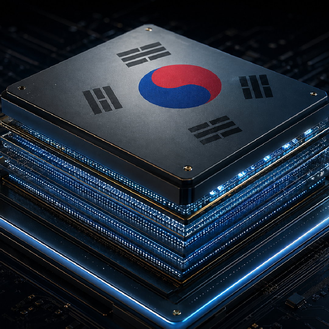

The production capacity for HBM4 — the high-bandwidth memory that powers AI accelerators — is already committed through the end of the decade. Orders placed in recent months by NVIDIA, AMD, and the major American hyperscalers have locked in the majority of available supply across multiple product cycles, leaving most European high-performance computing projects with no allocation at the table.
The supply constraint is structural. SK hynix and Samsung Electronics together control the overwhelming share of global High Bandwidth Memory production, and their Icheon and Pyeongtaek facilities are fully booked for the next three product generations. The real bottleneck, however, is not DRAM fabrication itself — it is advanced CoWoS packaging capacity, concentrated in a handful of Asian sites and still running below demand.
What changes with HBM4
HBM4 doubles the interface width compared to HBM3E, moving from a 1024-bit bus to 2048 bits per stack. This brings bandwidth above 1.6 terabytes per second per stack, with 16-Hi configurations reaching 36 gigabytes of capacity. Alongside the bandwidth gain, the architecture delivers roughly 30% better energy efficiency at equivalent throughput — a relevant figure for hyperscale data centers where memory power consumption accounts for a significant share of total rack draw.
The more significant architectural change is in the base die. SK hynix has moved production of the HBM4 base die to TSMC, using 5 and 12 nm logic nodes to embed advanced functions directly into the memory stack: power delivery management, near-memory and in-memory compute capability, and structured debug. This decision tightly couples SK hynix's product roadmap to TSMC wafer availability — and signals that high-performance memory can no longer be designed in isolation from logic.
A supply chain locked through 2029
NVIDIA has committed a substantial share of SK hynix's HBM4 production capacity for the Vera Rubin accelerator platform. AMD has signed a multi-year agreement with Samsung for HBM4 supply destined for the MI400 Instinct family. Google, Amazon, and Microsoft complete the picture with allocations for their respective proprietary accelerators — TPUs, Trainium, and Maia.
European allocation, by contrast, is marginal. No EuroHPC consortium project holds meaningful direct contracts with either Korean supplier. European industrial operators — from electronic test equipment to radar systems, from high-end oscilloscopes to particle physics data acquisition platforms — are effectively queued behind the large American clients. The practical consequence is a lead time exceeding eighteen months and unit prices carrying a significant premium over early-2025 estimates.
The advanced packaging constraint
Advanced CoWoS packaging from TSMC is the actual chokepoint. It is the only technology available in volume that allows HBM stacks to be co-integrated with an AI accelerator on a silicon interposer. TSMC has expanded CoWoS capacity significantly, but it remains below demand. Samsung is developing its own advanced packaging line at Cheonan, expected to reach volume in the second half of 2026, with yields still to be validated. Intel Foundry offers EMIB as an alternative, but current volumes are oriented primarily toward its own accelerator roadmap.
In Europe, advanced packaging for HBM is essentially absent. The German and French facilities of Infineon, STMicroelectronics, and Bosch operate on packaging technologies oriented toward power management, automotive, and analog applications. The joint TSMC-Bosch-Infineon-NXP fab in Dresden, entering production in 2027, is dimensioned for 12 and 28 nm automotive applications — not for logic-memory advanced packaging. The technology gap in this specific segment between Asia and Europe is estimated at seven to eight years.
The industrial implications
The downstream effects are significant. European manufacturers integrating HBM-based FPGAs or accelerators into scientific and industrial systems must now plan procurement two years in advance or accept components on shorter availability windows. For small-series production, unit costs have become difficult to absorb: an accelerator with 192 GB of HBM3E that cost approximately €25,000 in the industrial segment in 2024 now consistently exceeds €38,000.
At the strategic level, the dependency on Korean memory compounds the existing dependency on Taiwanese logic and American chip architectures. The European Commission is evaluating strategic stockpiling measures under the Critical Raw Materials Act, but HBM falls in a regulatory grey zone — it is a system component, not a raw material, and is not explicitly covered. The situation is further complicated by Chinese export controls on critical materials and US Section 232 tariffs, which affect the same supply chain at multiple points.
What this means for chip design
The HBM4 constraint has a direct implication for how custom silicon projects should be structured going forward. Designs that integrate high-bandwidth memory need to account for memory availability as a primary architectural constraint — not a procurement afterthought. This means evaluating GDDR7 as an alternative where bandwidth requirements permit, decoupling architectures from a specific memory generation wherever possible, and building supply risk into multi-year design roadmaps from the earliest stages.
For Move Silicon, this supply dynamic confirms a direction the company has been building toward: helping design teams reduce the time between architectural decisions and working silicon. When memory constraints, packaging bottlenecks, and allocation windows compress the margin for iteration, the ability to move faster through the design cycle becomes a competitive advantage. The tools and methodologies Move Silicon brings to custom ASIC and IP design are precisely what allows teams to respond to a hardware landscape that is increasingly defined by external supply constraints rather than internal design timelines.
